

How Sanjay Mehrotra Put Micron in a League with Samsung and SK Hynix
By JL Zhang | 19 May, 2026
The Micron CEO used his engineering virtuosity to achieve a 30% power-efficiency edge, placing Micron ahead in the 3-way AI HBM race.
For most of its history Micron Technology was the memory industry's also-ran — the American company that perpetually chased Samsung and SK Hynix without ever quite catching them. It survived the brutal memory wars of the 1980s and 1990s that wiped out dozens of competitors, then spent decades playing catch-up on process nodes while the Korean giants set the pace.
Today, that story has been completely rewritten. Micron holds roughly 21% of the global high-bandwidth memory market, it's sold out through 2026, its gross margins on AI memory have touched 66%, and its market cap has surged past $800 billion. The man most responsible for this transformation is Sanjay Mehrotra — an engineer-turned-CEO who arrived in 2017 with a clear doctrine and the patience to execute it over years before the payoff became obvious.
An Engineer Takes the Wheel
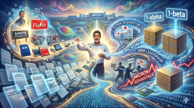
Mehrotra's background matters enormously to understanding what he did at Micron. He didn't come from finance or operations. He co-founded SanDisk in 1988 — a flash memory startup — and led it for nearly three decades, holding more than 70 patents, several of which are foundational to high-capacity flash memory. He grew SanDisk into a Fortune 500 company before Western Digital acquired it in 2016. When Micron's board recruited him in 2017, they weren't hiring a cost-cutter. They were hiring someone who understood, at a cellular level, that in memory semiconductors, the company with the most advanced manufacturing process wins on margin regardless of volume.
That insight became the cornerstone of everything he did next.
The company he inherited wasn't in crisis, but it wasn't leading either. Micron had made a smart acquisition in 2013 — the bankrupt Japanese manufacturer Elpida Memory — for roughly $2 billion. That deal doubled Micron's production capacity, secured Apple supply chain relationships, and handed Micron a world-class 300mm fab in Hiroshima that had been Elpida's crown jewel. But integrating Elpida's processes into Micron's existing technology base proved difficult and time-consuming. Through the mid-2010s, Micron was still, in its own engineers' words, "always trying to close the gap instead of trying to get technology leadership."
Mehrotra's first major decision was to stop closing the gap and start opening one.
The "Value Over Volume" Shift
In an industry historically obsessed with market share and wafer output, Mehrotra made an almost contrarian bet: he'd pursue technology leadership and high-margin products instead of flooding the market with commodity chips. He called it "value over volume." Rather than competing on price by scaling production, Micron would compete on process node advancement, win premium customers, and let the margins follow.
This meant pouring investment into R&D and manufacturing transformation — billions of dollars to upgrade fabs, automate production, and accelerate the cadence of process node transitions. It also meant accepting that Micron wouldn't win on volume in the short run, and trusting that being first to the most advanced nodes would eventually command a pricing premium that more than compensated.
The first sign it was working came in 2021, when Micron became the first company in the world to ship DRAM manufactured on its 1α (1-alpha) process node — beating Samsung and SK Hynix by roughly a year. That was a genuine milestone. For the first time in its history, Micron wasn't catching up. It was leading. The institutional confidence that came from that win was crucial: it proved the strategy worked, and it set up the even more important victory that followed.
The 1β Breakthrough
In November 2022, Micron announced mass production readiness for its 1β (1-beta) DRAM node — again, the first in the world to reach that milestone. The 1β node delivered a 15% power efficiency improvement and more than 35% better bit density compared to 1α. Smaller transistors, finer circuits, lower operating voltage. Micron manufactured it at the Hiroshima fab it had inherited from Elpida, which by this point it had fully integrated and upgraded into one of the most advanced DRAM facilities on earth.
What made 1β especially significant wasn't just the node itself — it was what Mehrotra chose to do with it. Instead of deploying 1β broadly across Micron's product portfolio to maximize bit output, he pointed it at the highest-value target available: high-bandwidth memory for AI accelerators. And rather than trying to compete with SK Hynix and Samsung across every HBM generation, he made a bold call to skip HBM3 and jump straight to HBM3E, using the power efficiency advantages that 1β made possible as the primary differentiator.
That decision turned out to be one of the shrewdest moves in recent semiconductor history.
The 30% Power Edge That Changed Everything
HBM3E built on 1β gave Micron something its competitors couldn't immediately match: chips that consumed roughly 30% less power than competing solutions. In most eras of chip history, a 30% power advantage would be notable. In 2024 and 2025, as AI data centers slammed into physical power constraints, it was decisive.
The economics of an AI data center are brutally simple. You can only draw so many megawatts from the grid. Every watt you save on memory is a watt you can spend on more compute. Hyperscalers building billion-dollar clusters were suddenly very interested in memory that ran cooler and drew less power — not just memory that was fast. Micron's HBM3E checked that box in a way SK Hynix's and Samsung's products didn't, and it wasn't an accident. It was the direct downstream consequence of being first to 1β, first to get smaller die sizes, and first to drive down the voltage requirements for AI memory.
The results were fast. Google, which had planned to use Samsung's HBM3E in its custom AI servers, switched to Micron after Samsung repeatedly failed Nvidia's thermal qualification tests. Nvidia itself qualified Micron's 12-layer HBM3E for its Blackwell Ultra GB300 platform. Micron's HBM market share, which had been in the low single digits as recently as 2024, climbed to 21% by mid-2025, overtaking Samsung to become the world's second-largest HBM supplier. Its entire 2026 HBM production sold out before the year began, including the next-generation HBM4.
Samsung's Stumble Was No Coincidence
It's worth being precise about why Samsung fell behind, because it makes clear that Micron's rise wasn't just a matter of luck or Samsung's misfortune. Samsung's HBM3E problems were rooted in packaging technology. Samsung insisted on a thermal compression approach called TC-NCF that, when applied to 12-layer stacks, produced heat accumulation and signal degradation that couldn't pass Nvidia's qualification. It failed qualification repeatedly throughout 2024 and didn't pass until September 2025 — by which point most supply contracts were already locked up.
Micron's cleaner power profile meant its HBM3E ran cooler inherently, making the packaging challenges more manageable. SK Hynix had its own proprietary packaging technology — MR-MUF — that handled heat well, which is why SK Hynix kept its dominant 60%+ market share throughout. But Micron's process advantage at the die level gave it a different path to meeting the same thermal requirements, one that Samsung's older node technology simply couldn't replicate quickly.
The Road Ahead
Mehrotra hasn't stopped. Micron's 1γ (1-gamma) node — the generation after 1β — is now ramping at the Hiroshima fab and Micron's Taiwan facilities, and it's the first company in Japan to use extreme ultraviolet lithography in production. HBM4 samples are already shipping to customers including Nvidia's Vera Rubin platform. Mehrotra has publicly projected the HBM market growing from roughly $35 billion in 2025 to $100 billion by 2028 — hitting that number two years earlier than Micron had previously forecast.
The company has also committed to a $200 billion U.S. manufacturing expansion, including two new fabs in Idaho and a massive facility in Clay, New York, designed to bring end-to-end HBM manufacturing onto American soil. Jensen Huang called it "an important step forward for the AI ecosystem." The CHIPS Act funding Mehrotra's team lobbied for will help underwrite those facilities.
None of this was inevitable. Memory is a brutal industry that's destroyed companies far larger and older than Micron. The Korean giants didn't stumble — SK Hynix in particular executed brilliantly, starting its HBM journey in 2006 and building a decade-long head start. Micron's achievement is that it found a different angle of attack: not earlier, but smarter. It built a process node advantage, deployed it against the one bottleneck — power — that mattered most to the customers who mattered most, and converted that into design wins that are now baked into multi-year supply agreements.
Mehrotra didn't get lucky. He made a series of disciplined, technically sophisticated bets — value over volume, 1α before anyone else, 1β before anyone else, HBM3 skip, HBM3E power focus — and each one compounded the last. The 30% power edge isn't a product feature. It's the accumulated output of eight years of deliberate choices by an engineer who understood exactly what game he was playing.
© 2026 by Asian Media Group Inc.
Recent Articles
- Intel Turns to Next-Gen ASML Tool to Help Make Its Laptop Chips
- Cambodian Gaming Tycoon Was Landlord to Chinese Scam Compound
- China New Home Price Slide Slows, but Recovery Doubtful
- Iran Threatens to Block More Vital Seaways as Trump Orders Renewed Iran Blockade
- ASML Beats Q2 Revenue Estimates on AI Chip Demand
- Nvidia Has Begun Shipping H200 AI Chips to China
- IBM Warns AI Boom Is Squeezing Software Budgets; Sending Shares Down
- Two Utah National Monuments Fall to Trump Anti-Green Drive
- 72% of Americans Disagree with Trump on Refugees
- June CPI Not As Hot As Feared, Soothing Markets