

How Likely Is IBM's Sub-Nanometer Chip to Scale into Production?
By Ben Lee | 30 Jun, 2026
A 0.7 angstrom chip going into mass production would represent a development deemed unlikely by the semiconductor industry.
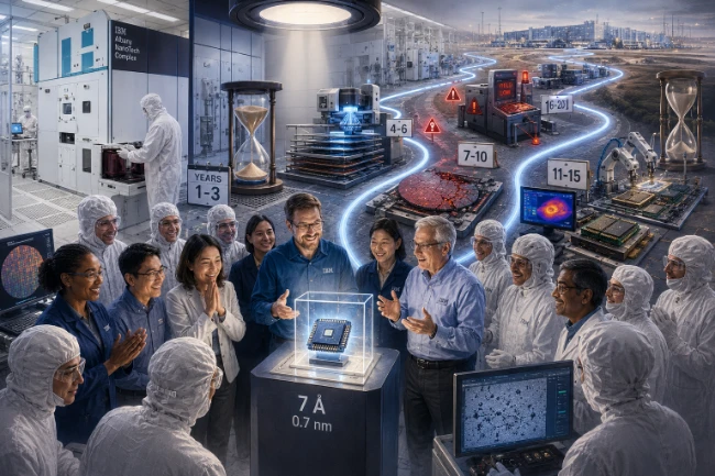
On June 25,2026 IBM researchers gathered at the company's Yorktown Heights headquarters to announce something the semiconductor industry had widely considered physically impossible: a working chip architecture at the 0.7-nanometer — or 7-angstrom — node.
To grasp the scale, consider that a human red blood cell is roughly 7,000 nanometers wide, making these transistors about 10,000 times smaller than a single blood cell. At this dimension, chip features are approaching the size of individual atoms. IBM has not merely crept past the one-nanometer threshold. It has leaped across it.
The announcement, delivered simultaneously with research presented at the VLSI 2026 symposium in Kyoto, marks a genuine inflection point — not because sub-nanometer chips will be in your laptop next year, but because IBM has demonstrated that the road ahead is open at a moment when much of the industry assumed it was closing.
What IBM Built and How
The architecture enabling this milestone is called nanostack. It is a logical evolution of the nanosheet transistor design that IBM itself pioneered and that now underpins most of the world's leading-edge chips, including those manufactured by TSMC, Samsung, and Intel. Where nanosheets are essentially flat arrangements of stacked silicon channels through which electrons flow under gate control, nanostack takes the concept vertical — stacking and staggering transistors in three dimensions through a process called 3D sequential integration.
Each transistor in the nanostack design comprises three nanosheet elements roughly five nanometers thick, spaced about nine nanometers apart. Each nanosheet consists of approximately 15 rows of silicon atoms. The bonding between layers uses an ultra-thin dielectric material, and critically, each stacked layer can use a different semiconductor channel material. This allows engineers to optimize the n-type and p-type transistors — NFET and PFET — independently, squeezing more performance and efficiency out of each device.
The result is a chip that packs nearly 100 billion transistors onto a surface the size of a fingernail — roughly twice the density of IBM's 2-nanometer chip unveiled in 2021, which at the time was itself the most advanced chip design in the world. IBM claims the 0.7-nm node delivers up to 50 percent more performance or up to 70 percent greater energy efficiency compared to that 2-nm predecessor.
The AI implications are striking. IBM Research estimates that an AI accelerator built on 7-angstrom technology could deliver approximately 7,000 trillion operations per second (TOPS), compared to roughly 1,500 TOPS on current hardware. If those projections hold, training a large frontier AI model — currently a three-month affair — could be cut to about two weeks.
IBM also presented separate VLSI 2026 research showing that the nanostack architecture achieves 40 percent greater density in SRAM, the fast on-chip memory that has become one of the primary bottlenecks in AI chip design. Between the 3-nm and 2-nm generations, SRAM density improved by only a few percent. A 40-percent leap in a single generation, if it translates to production, would be arguably as important as the transistor-density headline.
Critically, IBM validated the architecture physically, not just on paper. Researchers demonstrated functional CMOS inverters — the basic building block of digital logic — exhibiting expected switching behavior, which confirms the structure can be built and can support real computation. The company described the experimental validation through ultra-thin dielectric bonding in CMOS integration and dual-channel engineering.
The Gap Between Demonstration and Production
The enthusiasm accompanying the announcement deserves a measured counterweight: this is a research demonstration, and a wide chasm separates a working prototype from a chip in mass production.
IBM no longer manufactures commercial chips at volume. The company sold its chip fabrication business to GlobalFoundries years ago and has since operated exclusively as a semiconductor research institution, developing foundational IP and then licensing or transferring it to manufacturing partners. That business model has yielded extraordinary scientific breakthroughs — and a persistent lag between discovery and deployment.
IBM's 2-nm chip is the clearest illustration. Unveiled with great fanfare in 2021, it promised 45 percent better performance or 75 percent greater energy efficiency compared to 7-nm chips. Five years later, that technology is only now approaching volume production — and not through IBM itself, but through Rapidus, a Japanese startup founded in 2022 with government backing and a partnership with IBM to bring 2-nm manufacturing to Japan. Rapidus opened its pilot production line in Chitose, Hokkaido in April 2025 and is targeting mass production of 2-nm chips by the second half of 2027. IBM has dispatched engineers to work alongside Rapidus staff, and the collaboration has made genuine technical progress on complex manufacturing challenges, including the multi-threshold voltage techniques required for 2-nm nanosheet transistors. But commercially available 2-nm chips from IBM-derived technology remain over a year away, even after half a decade.
Against that backdrop, IBM's projection that nanostack could reach production "within five years" — placing earliest commercial availability around 2031 — looks optimistic rather than conservative.
The Physical and Engineering Challenges of Going Sub-Nanometer
The difficulties of getting from a lab demonstration to a shipping product at 0.7 nanometers are substantial, and they compound the already formidable challenges that have plagued 2-nm production ramps at Samsung and Intel.
The most immediate obstacle is lithography. Printing circuit features at sub-nanometer scales requires High Numerical Aperture Extreme Ultraviolet lithography — High-NA EUV — the successor to the standard EUV tools that ASML currently sells to TSMC and others. High-NA EUV machines are enormously expensive (ASML's newest tool is priced at roughly $400 million per unit), slow to produce, and still being refined. IBM and its partners at the Albany NanoTech Complex — including Lam Research and Tokyo Electron — are working to develop process recipes for these tools, but the technology remains in early stages industry-wide.
The 3D stacking approach that makes nanostack possible introduces a further complication that engineers call the thermal budget problem. Each additional layer of transistors must be built without exceeding approximately 400°C, the temperature at which the dielectric bonds holding lower layers together begin to degrade. Managing heat across multiple stacked tiers while maintaining precise material properties is a challenge with no fully mature solution.
There is also the yield problem. Semiconductor fabrication is an exercise in controlled imperfection. Even at 2 nm, Samsung's early yields reportedly fell in the 50 to 60 percent range, meaning roughly half of all chips produced were defective. When transistors are stacked in two tiers, as the nanostack architecture requires, a defect in either layer renders the entire chip unusable. As one MIT researcher noted in commentary on the announcement, manufacturing failure rates will be inherently higher for multi-tier designs, and that will be costly.
Finally, the EDA software that chip designers use to create and verify circuits does not yet exist for 3D transistor-level design. IBM has acknowledged that the necessary tools "need to arrive" — an honest admission that an entirely new category of software infrastructure must be developed before nanostack chips can be commercially designed, let alone manufactured.
IBM's Strategy and the Competitive Landscape
Despite these challenges, IBM's announcement is a genuine strategic statement, not mere theater. The company's historical role — pioneering transistor architectures that later become industry standard — has proven durable. The nanosheet technology that TSMC, Samsung, and Intel now use in their leading-edge 2-nm and 1.8-nm processes originated in IBM's research labs, developed at the Albany NanoTech Complex years before any foundry deployed it in production.
The competitive context around IBM's announcement is revealing. TSMC began volume production of its 2-nm N2 process in Q4 2025 and is ramping toward 100,000 wafers per month in 2026, with Apple having secured more than half of the initial capacity. Intel's 18A-P process, an enhanced 1.8-nm node using RibbonFET gate-all-around transistors and backside power delivery, entered risk production in June 2026. TSMC's 1.4-nm A14 node is on track for 2028. IBM's 0.7-nm nanostack is at least two full generations ahead of anything any foundry is currently shipping — but it exists only as a validated prototype.
The commercialization path is also undefined in ways that matter. IBM has not named a manufacturing partner for nanostack. Its previous alliance with Rapidus was designed around 2-nm technology, and Rapidus is one of the few organizations anywhere currently running a High-NA EUV tool, which gives IBM's Albany consortium a potential advantage in co-developing the process recipes nanostack will eventually require. But IBM Research VP Jay Gambetta has said the company's near-term focus remains helping partners scale today's 2-nm nanosheet technology — which means nanostack commercialization, whenever it begins, starts from a later date than the announcement suggests.
An Open Question
So how likely is IBM's sub-nanometer chip to come to fruition? The honest answer is: more likely than skeptics will claim, and more slowly than enthusiasts will hope.
The physics is validated. The architecture is not a simulation or a projection — IBM has built working transistors and functioning logic circuits at the 0.7-nm node, peer-reviewed at a major symposium. That matters enormously. The semiconductor industry has a long tradition of dismissing as physically impossible what IBM's research labs then proceed to build.
The commercialization, however, depends on factors that are partly outside IBM's control: the maturation of High-NA EUV lithography, the development of 3D chip design software, the resolution of thermal and yield challenges, and the willingness of a major foundry partner to commit the billions of dollars required to build nanostack-compatible fabs. IBM's 2-nm track record — five years from announcement to still-not-fully-commercialized — suggests that 2031 is an aspirational timeline rather than a floor.
What is not in doubt is the significance of the demonstration itself. By proving that chip scaling can extend into the angstrom era, IBM has widened the horizon of what computation can become — and handed the industry a credible blueprint for the next decade of progress, even if the construction work lies largely ahead.
© 2026 by Asian Media Group Inc.
Recent Articles
- US-EU Trade Hits Record High Despite Tariff Tensions, Study Shows
- Chinese Independent Refiners Snap up Discounted Mideast Oil as Supplies Rise
- US Oil Companies See Big Profit Jump, Faces Pressure to Cut Pump Prices
- Drug Gangs Use Social Media to Recruit Thai Air Crew as Couriers
- Ghonhee Lee's Katalyst Launches Orbital Rescue Mission for NASA Satellite
- Zuckerberg Says Meta AI Agent Tech Progressing Slower Than Expected
- Japan's Services Activity Returned to Growth in June
- Air Force to Investigate Officer Who Called for Trump Impeachment
- How Americans Plan to Celebrate July 4th 250
- Tesla's China-Made EV Sales Jumped 24.4% on Year in June